Every phone, car and data centre depends on chips holding billions of microscopic switches. It is tempting to picture them assembled by tiny machines, but that is not how it works. They are printed with light, in a process called chip lithography. How well the light behaves largely determines how small and how precise the circuits can be.
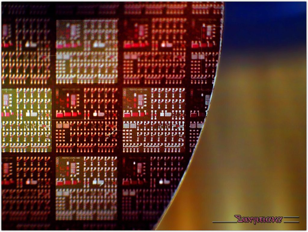
Understanding chip lithography explains a surprising amount about why the industry spends so much on a single machine.
How printing circuits with light works
The idea behind chip lithography resembles photography. A silicon wafer is coated with a light-sensitive layer. Light shines through a patterned plate called a mask, which holds the design, and an optical system shrinks that pattern onto the wafer. Where the light lands, the coating changes.
The wafer is then treated with chemicals that remove either the exposed or unexposed parts, leaving a pattern. Other steps add or etch materials. A modern chip needs this cycle repeated many times, layer on layer, with each layer lined up to the one beneath with extraordinary accuracy.
Because chip lithography is repeated so often, small improvements matter. A tiny gain in precision or speed multiplies across layers, wafers and factories.
Scale helps put this in perspective. The features on a modern chip are far smaller than a wavelength of visible light, which is why clever optics and special illumination are needed even before shorter wavelengths enter the picture. It is a bit like painting a fine portrait with a brush much wider than the details you want.
Resolution is also helped by the numerical aperture of the optics, which describes how much light the lens system collects. Bigger optics resolve finer detail, but they are harder to build and align.
Why wavelength matters
Light behaves like a wave, and the size of the smallest feature you can print is tied to its wavelength. Shorter wavelengths can draw finer details, in the same way a thin pen draws finer lines than a thick marker.
Over the years, chip lithography moved to shorter and shorter wavelengths of light. Engineers also used clever tricks to squeeze more detail from each wavelength, including special lenses, patterns designed to correct for blurring, and exposing a layer in multiple passes.
Those tricks work, but they add steps, cost and complexity. That is a big reason the industry has long wanted light sources with much shorter wavelengths, so fewer workarounds are needed.
Masks used in chip lithography are remarkable objects. They must be free of tiny defects, since any flaw is copied onto every chip. Inspection and repair of masks is a whole industry, and the cost of making a set for an advanced chip is one reason only high-volume products justify the newest processes.

Chip lithography: the light source problem
Making extremely short-wavelength light is hard. Such light is absorbed by almost everything, including air and glass, so the machines must operate in a vacuum and use mirrors rather than lenses. Generating enough of it with steady power is a big engineering challenge in itself.
The more powerful and stable the light, the faster wafers can be exposed and the more chips come out per hour. Ideas for better chip lithography light sources keep appearing in research labs and company announcements, including new approaches based on particle accelerators or lasers.
Turning a laboratory demonstration into a reliable chip lithography tool is another matter. Machines must run for long periods, with very high uptime and low cost per wafer. Many promising technologies do not make that jump.
Supply chains matter as well. Light sources depend on specialised lasers, mirrors, materials and gases, and each of these comes from a limited set of suppliers. A delay in one part can slow down an entire factory, which is why partnerships across companies and countries are so common in this field.

Why governments care, and how to judge big claims
Advanced chips support computing, communications, medicine and defence, so countries treat chipmaking capacity as strategic. The equipment is complex and made by a very small number of firms, which makes it a subject of trade policy and export rules.
When you see an announcement about a new light source or chip lithography method, ask grounded questions. Is it a lab result or a production tool? What power or throughput was shown? Has it been tested in a real factory? What does it cost? Who else needs to change their materials and processes for it to work?
Be wary of headlines promising to overturn the industry overnight. Progress here tends to be incremental and slow. Still, it is worth following, because the quality of the light quietly shapes what future devices can do.
For ordinary readers, the takeaway is that chip progress is not only a matter of clever circuit design. It is also physics, optics and manufacturing discipline working together. When a new phone or processor boasts about smaller features, light is a big part of the reason it was possible.
For wider context on chip lithography, the Wikipedia article on photolithography is a neutral place to start. To keep reading here, try What a Startup Valuation Really Means, and Why Fintech Companies Get Valued So High or When Robot Vacuum Makers Cut Jobs: What It Means for Owners and the Gadget Market.
A useful habit is to separate three questions whenever you read about chips: what was demonstrated, what is in production, and what is only planned. They often differ by years.